- 您现在的位置:买卖IC网 > Sheet目录3880 > PIC16F1933-I/ML (Microchip Technology)IC MCU 8BIT FLASH 28-QFN
2009 Microchip Technology Inc.
DS39637D-page 137
PIC18F2480/2580/4480/4580
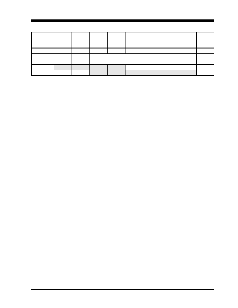
TABLE 11-2:
SUMMARY OF REGISTERS ASSOCIATED WITH PORTA
Name
Bit 7
Bit 6
Bit 5
Bit 4
Bit 3
Bit 2
Bit 1
Bit 0
Reset
Values
on Page:
PORTA
RA7(1)
RA6(1)
RA5
RA4
RA3
RA2
RA1
RA0
LATA
LATA7(1)
LATA6(1) LATA Output Latch Register
TRISA
TRISA7(1) TRISA6(1) PORTA Data Direction Register
ADCON1
—
VCFG1
VCFG0
PCFG3
PCFG2
PCFG1
PCFG0
CVRCON(2)
CVREN
CVROE
CVRR
CVRSS
CVR3
CVR2
CVR1
CVR0
Legend: — = unimplemented, read as ‘0’. Shaded cells are not used by PORTA.
Note 1:
RA<7:6> and their associated latch and data direction bits are enabled as I/O pins based on oscillator
configuration; otherwise, they are read as ‘0’.
2:
These registers are unimplemented on PIC18F2X80 devices.
发布紧急采购,3分钟左右您将得到回复。
相关PDF资料
PIC16F785-I/ML
IC PIC MCU FLASH 2KX14 20QFN
XF2L-0425-1
CONN FPC 4POS 0.5MM SMT
PIC16F1933-I/MV
IC MCU 8BIT FLASH 28-UQFN
PIC16F785-I/SO
IC PIC MCU FLASH 2KX14 20SOIC
PIC16C56A-04/SO
IC MCU OTP 1KX12 18SOIC
PIC18F23K20-I/MV
IC MCU 8BIT 8KB FLASH 28UQFN
PIC16F627A-I/P
IC MCU FLASH 1KX14 EEPROM 18DIP
XF2G-1414-11
CONN FPC 14POS 0.5MM SMT
相关代理商/技术参数
PIC16F1933-I/MV
功能描述:8位微控制器 -MCU 7KB Flash 256B RAM LCD 1.8-5.5V RoHS:否 制造商:Silicon Labs 核心:8051 处理器系列:C8051F39x 数据总线宽度:8 bit 最大时钟频率:50 MHz 程序存储器大小:16 KB 数据 RAM 大小:1 KB 片上 ADC:Yes 工作电源电压:1.8 V to 3.6 V 工作温度范围:- 40 C to + 105 C 封装 / 箱体:QFN-20 安装风格:SMD/SMT
PIC16F1933-I/SO
功能描述:8位微控制器 -MCU 7KB Flash 1.8-5.5V 256B RAM 256B EEPROM RoHS:否 制造商:Silicon Labs 核心:8051 处理器系列:C8051F39x 数据总线宽度:8 bit 最大时钟频率:50 MHz 程序存储器大小:16 KB 数据 RAM 大小:1 KB 片上 ADC:Yes 工作电源电压:1.8 V to 3.6 V 工作温度范围:- 40 C to + 105 C 封装 / 箱体:QFN-20 安装风格:SMD/SMT
PIC16F1933-I/SP
功能描述:8位微控制器 -MCU 7KB Flash 1.8-5.5V 256B RAM 256B EEPROM RoHS:否 制造商:Silicon Labs 核心:8051 处理器系列:C8051F39x 数据总线宽度:8 bit 最大时钟频率:50 MHz 程序存储器大小:16 KB 数据 RAM 大小:1 KB 片上 ADC:Yes 工作电源电压:1.8 V to 3.6 V 工作温度范围:- 40 C to + 105 C 封装 / 箱体:QFN-20 安装风格:SMD/SMT
PIC16F1933-I/SS
功能描述:8位微控制器 -MCU 7KB Flash 1.8-5.5V 256B RAM 256B EEPROM RoHS:否 制造商:Silicon Labs 核心:8051 处理器系列:C8051F39x 数据总线宽度:8 bit 最大时钟频率:50 MHz 程序存储器大小:16 KB 数据 RAM 大小:1 KB 片上 ADC:Yes 工作电源电压:1.8 V to 3.6 V 工作温度范围:- 40 C to + 105 C 封装 / 箱体:QFN-20 安装风格:SMD/SMT
PIC16F1933T-I/ML
功能描述:8位微控制器 -MCU 7KB Flash 1.8-5.5V 256B RAM 256B EEPROM RoHS:否 制造商:Silicon Labs 核心:8051 处理器系列:C8051F39x 数据总线宽度:8 bit 最大时钟频率:50 MHz 程序存储器大小:16 KB 数据 RAM 大小:1 KB 片上 ADC:Yes 工作电源电压:1.8 V to 3.6 V 工作温度范围:- 40 C to + 105 C 封装 / 箱体:QFN-20 安装风格:SMD/SMT
PIC16F1933T-I/MV
功能描述:8位微控制器 -MCU 7KB Flash 256B RAM LCD 1.8-5.5V RoHS:否 制造商:Silicon Labs 核心:8051 处理器系列:C8051F39x 数据总线宽度:8 bit 最大时钟频率:50 MHz 程序存储器大小:16 KB 数据 RAM 大小:1 KB 片上 ADC:Yes 工作电源电压:1.8 V to 3.6 V 工作温度范围:- 40 C to + 105 C 封装 / 箱体:QFN-20 安装风格:SMD/SMT
PIC16F1933T-I/SO
功能描述:8位微控制器 -MCU 7KB Flash 1.8-5.5V 256B RAM 256B EEPROM RoHS:否 制造商:Silicon Labs 核心:8051 处理器系列:C8051F39x 数据总线宽度:8 bit 最大时钟频率:50 MHz 程序存储器大小:16 KB 数据 RAM 大小:1 KB 片上 ADC:Yes 工作电源电压:1.8 V to 3.6 V 工作温度范围:- 40 C to + 105 C 封装 / 箱体:QFN-20 安装风格:SMD/SMT
PIC16F1933T-I/SS
功能描述:8位微控制器 -MCU 7KB Flash 1.8-5.5V 256B RAM 256B EEPROM RoHS:否 制造商:Silicon Labs 核心:8051 处理器系列:C8051F39x 数据总线宽度:8 bit 最大时钟频率:50 MHz 程序存储器大小:16 KB 数据 RAM 大小:1 KB 片上 ADC:Yes 工作电源电压:1.8 V to 3.6 V 工作温度范围:- 40 C to + 105 C 封装 / 箱体:QFN-20 安装风格:SMD/SMT